- 您现在的位置:买卖IC网 > Sheet目录3833 > AT87251G2D-3CSUM (Atmel)IC 8051 MCU 32K OTP 24MHZ 40DIP
12
AT/TSC8x251G2D
4135F–8051–11/06
compatibility with the C51 Architecture). When PC increments beyond the end of seg-
ment FE:, it continues at the reset address FF:0000h (linearity). When PC increments
beyond the end of segment 01:, it loops to the beginning of segment 00: (this prevents
from its going into the reserved area).
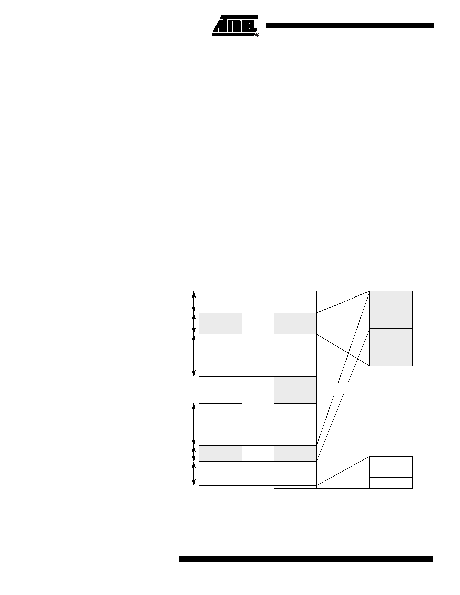
Data Memory
The TSC80251G2D derivatives implement 1 Kbyte of on-chip data RAM. Figure 5
shows the split of the internal and external data memory spaces. This memory is
mapped in the data space just over the 32 bytes of registers area (see TSC80251 Pro-
grammers’ Guide). Hence, the part of the on-chip RAM located from 20h to FFh is bit
addressable. This on-chip RAM is not accessible through the program/code memory
space.
F o r f a st er com put atio n w i th t he on- chip R O M / EPR O M cod e o f the
TSC83251G2D/TSC87251G2D, its upper 16 KB are also mapped in the upper part of
the region 00: if the On-Chip Code Memory Map configuration bit is cleared (EMAP# bit
in UCONFIG1 byte, see Figure ). However, if EA# is tied to a low level, the
TSC80251G2D derivative is running as a ROMless product and the code is actually
fetched in the corresponding external memory (i.e. the upper 16 KB of the lower 32 KB
of the segment FF:). If EMAP# bit is set, the on-chip ROM is not accessible through the
region 00:.
All the accesses to the portion of the data space with no on-chip memory mapped onto
are redirected to the external memory.
Figure 5.
Data Memory Mapping
On-chip ROM/EPROM
Code Memory
Data Segments
Data External
Memory Space
16 KB
EA# = 0
EA# = 1
32 KB
Reserved
64 KB
47 KB
FF:FFFFh
FF:8000h
FF:7FFFh
FF:0000h
FE:FFFFh
FE:0000h
FD:FFFFh
01:FFFFh
01:0000h
02:0000h
00:FFFFh
00:0420h
32 bytes reg.
RAM Data
1 Kbyte
16 KB
00:C000h
00:BFFFh
EMAP# = 1
EMAP# = 0
16 KB
64 KB
发布紧急采购,3分钟左右您将得到回复。
相关PDF资料
AT80C51RA2-SLSUM
IC 8051 MCU ROMLESS 44PLCC
AT80C51RA2-SLSUL
IC 8051 MCU ROMLESS 44PLCC
AT80C51RA2-RLTUM
IC 8051 MCU ROMLESS 44VQFP
213931-5
CONN JACKSCREW RECEPT 34 POS
AT80C51RA2-RLTUL
IC 8051 MCU ROMLESS 44VQFP
AT80C51RA2-3CSUM
IC 8051 MCU ROMLESS 40DIP
AT80C51RA2-3CSUL
IC 8051 MCU ROMLESS 40DIP
AT80C31X2-SLSUM
IC 8031 MCU ROMLESS 44PLCC
相关代理商/技术参数
AT87251G2D-RLTUL
制造商:ATMEL 制造商全称:ATMEL Corporation 功能描述:B/16-BIT MICROCONTROLLER WITH SERIAL COMMUNICATION INTERFACES
AT87251G2D-RLTUM
功能描述:8位微控制器 -MCU 251G2D 8/16bitC OTP 5V RoHS:否 制造商:Silicon Labs 核心:8051 处理器系列:C8051F39x 数据总线宽度:8 bit 最大时钟频率:50 MHz 程序存储器大小:16 KB 数据 RAM 大小:1 KB 片上 ADC:Yes 工作电源电压:1.8 V to 3.6 V 工作温度范围:- 40 C to + 105 C 封装 / 箱体:QFN-20 安装风格:SMD/SMT
AT87251G2D-SLSUL
功能描述:8位微控制器 -MCU Microcontroller
RoHS:否 制造商:Silicon Labs 核心:8051 处理器系列:C8051F39x 数据总线宽度:8 bit 最大时钟频率:50 MHz 程序存储器大小:16 KB 数据 RAM 大小:1 KB 片上 ADC:Yes 工作电源电压:1.8 V to 3.6 V 工作温度范围:- 40 C to + 105 C 封装 / 箱体:QFN-20 安装风格:SMD/SMT
AT87251G2D-SLSUM
功能描述:8位微控制器 -MCU OTP 8/16bit St 5V 24MHz RoHS:否 制造商:Silicon Labs 核心:8051 处理器系列:C8051F39x 数据总线宽度:8 bit 最大时钟频率:50 MHz 程序存储器大小:16 KB 数据 RAM 大小:1 KB 片上 ADC:Yes 工作电源电压:1.8 V to 3.6 V 工作温度范围:- 40 C to + 105 C 封装 / 箱体:QFN-20 安装风格:SMD/SMT
AT875
制造商:POSEICO 制造商全称:POSEICO 功能描述:PHASE CONTROL THYRISTOR
AT875LT
制造商:POSEICO 制造商全称:POSEICO 功能描述:PHASE CONTROL THYRISTOR
AT875LTS44
制造商:POSEICO 制造商全称:POSEICO 功能描述:PHASE CONTROL THYRISTOR
AT875S44
制造商:POSEICO 制造商全称:POSEICO 功能描述:PHASE CONTROL THYRISTOR